Perfluorinated Compounds
European industry remains at forefront of greenhouse gas emissions reduction
The European Semiconductor Industry Association (ESIA) announced in May 2021 that the industry has achieved a 42% absolute emission reduction of ‘perfluorocompound’ gases from 2010 to 2020. PFCs are greenhouse gases which are used in the semiconductor manufacturing process. The sector’s emission reductions show a strong voluntary commitment to fight climate change and was achieved through substantial investment to implement reduction practices at operations across Europe. Over the same period, the industry has also reduced its overall emissions – normalised per unit of production index – by 54%. If no progressive action and investments had been undertaken by industry to reduce these emissions, they would have increased significantly under a business as usual scenario.
As the European Union is reviewing its climate legislation and fluorinated gas regulation , this leadership highlights the benefits and results of having a proactive approach from industry stakeholders. European PFC reduction efforts began in the mid-1990’s to address emissions. Previously, the European goal was to reduce by 2010 the absolute PFC emissions of the European semiconductor industry by 10% below the baseline year of emissions in 1995. The European semiconductor industry met and surpassed that voluntary reduction goal by reducing emissions by 41% below the 1995 baseline in 2010.
European semiconductor ‘perfluorocompound’ gas emissions 2010-2022
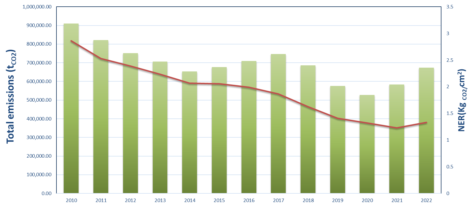
The PFC emission reductions pictured above have been achieved through the aggressive implementation of process optimisation and more efficient alternative processes, use of alternative chemistries and the installation of abatement equipment in Europe-based facilities. The industry remains dedicated to managing its PFC emissions, and continues to make reduction toward.
Global Management of PFC Gases
The management of PFC gas emissions through a global industry PFC goal is coordinated through an organisation called the World Semiconductor Council (WSC), consisting of regional semiconductor trade associations in Europe (ESIA), China, Chinese Taipei, Japan, Korea and United States who contribute to this worldwide reduction effort. ESIA is member to the WSC since 1997. It is important to outline that, through the WSC, the semiconductor industry was the first industry to align globally and establish a worldwide greenhouse gas emission goal which goes beyond the targets established by the Kyoto Protocol for Annex 1 countries.
In 2011, the WSC also announced a second voluntary PFC agreement for the next 10 years to 2020. The elements of the 2020 goal include the following:
- The implementation of best practices for new semiconductor fabs. The industry expects that the implementation of best practices will result in a Normalised Emission Rate (NER) in 2020 equivalent to a 30% NER reduction from 2010 aggregated baseline. Best practices will be continuously reviewed and updated by the WSC.
- The addition of “Rest of World” fabs (fabs located outside the WSC regions that are operated by a company from a WSC association) in reporting of emissions and the implementation of best practices for new fabs.
- A NER based measurement in kilograms of carbon equivalents per area of silicon wafers processed (KgCO2e/cm2) that will be a single WSC goal at the global level.
The WSC agreed to report its progress publicly on this new voluntary agreement on an annual basis in the WSC Joint Statement. These figures represent combined emissions for the six WSC regional associations, in their own regions and in the “Rest of World” fabs described above. In addition, to improve transparency, the WSC has made its Best Practices for PFC Reduction document available previously on the WSC website.
Useful Links
2021
ESIA brochure: the semiconductor industry, a key enabler of the reduction of carbon emissions
In September, ESIA published a brochure entitled “European Semiconductor Industry: A strong contributor to reducing Carbon Emissions” to outline the smart solution improvements enabled by semiconductors in areas such as automobiles, smarter mobility solutions (hybrid and electric vehicles), buildings, lighting, industry production, cloud storage and computing, and by facilitating the use of renewable energy sources.
Download the brochure here
European semiconductor industry continues to reduce its PFC emissions
In May, ESIA announced that the Eurpean semiconductor industry has achieved a 42% absolute emission reduction of perfluorocompound gases from 2010 to 2020. Over the same period, the industry has also reduced its overall emissions – normalised per unit of production index – by 54%.
Read more
2017
Update of the Best Practice Guidance of PFC Emission Reduction
As part of the 2016 data reporting on PFC emissions, the WSC has also revised its best practices document and published this update on the WSC website. The 2016 reporting also includes data on newly used gases such as CH2F2, C4F6, C5F8 and C4F8O. In addition, the WSC now reports the individual gas breakdowns.
Read more
2012
Best Practice Guidance of PFC Emission Reduction
To improve transparency, the WSC has made its Best Practices for PFC Reduction document available on the WSC website.
Read more
2011
ESIA PFC Voluntary Agreement Final Report-November 2011
This final report of the European Semiconductor Industry Association (ESIA) details the industry's voluntary actions from 1995 to 2010 to reduce emissions of PFCs and present 2010 data for the voluntary reduction programme. has surpassed the voluntary PFC goal by reducing absolute emissions by 41% below the 1995 baseline level.
Read more
2007
ESIA 2006 Intermediate Report on reduction of PFC emissions from European semiconductor manufacturing
The EECA-ESIA goal is to reduce by 2010 the ABSOLUTE PFC emissions of the European industry by 10% below the baseline year of emissions in 1995. If no progressive action and investments had been undertaken by the European industry to reduce emissions, these would have increased significantly more than 1995 levels under a business as usual scenario.
Read more
2005
Semiconductor manufacturers reduce PFC emissions
The world’s semiconductor manufacturers are on track to achieve their goal of reducing atmospheric emissions of perfluorocompounds (PFCs) to 10 percent below baseline levels by 2010, according to the World Semiconductor Council (WSC). PFCs have been identified as global warming gases.
Read more:
Applications
PFCs are used in semiconductor fabrication plants because they provide a uniquely effective process performance when etching and are a safer, more reliable source of fluorine, which is required for cleaning certain deposition process chambers. Manufacturers of semiconductor devices have been able to reduce PFC emissions by taking a number of actions including process optimization, use of alternative chemicals, employment of alternative manufacturing processes and improved abatement systems. However, the use of PFC gases in these processes is crucial to the production of semiconductor devices, as there are no effective substitutes outside the fluorinated chemistries that could be used effectively.
Perfluorinated gases are used in a number of different process steps.
- PFCs are used as etching gases for plasma etching. The gases etch the submicron patterns on metal and dielectric layers of advanced integrated circuits. In addition, SF6 decomposed by the plasma allows the etching chambers to be cleaned.
- The fluorinated compounds are also used to accurately perform a rapid chemical cleaning of Chemical Vapor Deposition (CVD) tool chambers. When the silicon and silicon based dielectric layers are being applied, a deposit remains in the CVD chamber. To ensure that the wafers do not become contaminated by these deposits, the chambers are cleaned at defined intervals, avoiding frequent mechanical wet cleanings.
- In the wafer testing process stage, SF6 is used as insulator for power device testing. Power device are used for automotive applications to simulate the real device working conditions which are essential to prove semiconductor device reliability. The SF6 reuse concept can allow SF6 to be used in an environmentally friendly manner and to be kept in a closed cycle.